RANDOM PAGE
SITE SEARCH
LOG
IN
SIGN UP
HELP
To gain access to revision questions, please sign up and log in.
A2
The AQA chip is a ...
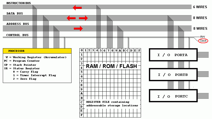
- Harvard Architecture (four bus) chip. It has an extra instruction bus.
This speeds up the chip because instructions and data can be fetched at the same time.
The traditional Von Neumann (three bus) chip has to fetch the instruction and the data in separate steps (slower).
- RISC chip (Reduced Instruction Set Chip). It has only 16 instructions.
Real-life microcontrollers from microchip.com have only 32 instructions.
The ARM Chip in most phones and tablets is a RISC chip.
CISC chips have a COMPLETE instruction set. They are much more complex and expensive and often usually than a similar RISC chip.

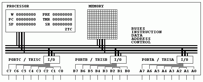
The processor contains ..
- an 8 bit unidirectional address bus. Data comes from the processor to other devices.
- an 8 bit bidirectional data bus. Data flows into and out of the processor.
- a 6 bit unidirectional instruction bus. Data flown into the processor.
- R/W is a unidirectional control bus line determining read or write operations.
- Clock is a unidirectional control bus line carrying the clock signal used to synchronise all the microcontroller operations.
Instruction and Operand Fetch
- Each instruction consists of a six bit op code and an eight bit operand.
- The op code is fetched on the instruction bus and, at the same time, the operand is fetched on the data bus.
Power-On and Reset
When the power is switched on, or after a reset, code execution starts from address 0x00.
The Registers, Buses, Memory and Input/Output

The Registers
- W is the working register or accumulator, through which all calculations are performed.
- PC is the program counter or instruction pointer.
This value (via the address bus) determines which instruction is fetched.
- SP is the stack pointer. It contains the stack pointer position.
When an interrupt or subroutine has completed, the processor returns to its previous task at the address held at the stack pointer position.
- The stack begins at R(0xF7) and grows towards zero.
Status Register and Flags
- SR is the status register containing status flags. These include ...
- Z (bit 2), the zero flag is set if there is a zero result in "W" after a calculation or move
- T (bit 1), the timer interrupt flag is set when the TMR register reaches zero.
- C (bit 0), the carry flag is set if a calculation gives a result too big to store in 8 bits (an overflow)
Timer and Prescaler Registers
- TMR is the timer register. This counts from any assigned number down to zero. When zero is reached, the T flag is set.
- TMR is decremented after a certain number of clock pulses determined by the PRE register.
- TMR is memory mapped at address R[0xFF].
- PRE is the prescaler. TMR is decremented when the number of counted clock pulses matches the value in PRE. This has the effect of dividing the clock frequency by (PRE + 1).
- If PRE is set to 0, TMR is disabled.
- If PRE is set to 1, the clock frequency is divided by 2. If PRE is 255, the clock frequency is divided by 256.
- PRE is memory mapped at address R[0xFE].
Configuring Input and Output Pins
- TRISA, TRISB, TRISC, PORTA, PORTB and PORTC are used for data input/output.
- The "tris" data direction registers control tristate logic used to determine whether the port pins are inputs or outputs.
- If a "tris" register bit is set to 1 then the equivalent port bit is an input.
- If the "tris" bit is set to 0 then the equivalent port bit is an output.
- The PORT and TRIS registers are memory mapped at addresses between R[0xF8]and R[0xFD].
- 1 = I = Input
- 0 = O = Output.
- All port pins default to Outputs because TRISA, B and C are initialised to Zero.
Memory
- R - there are 256 general purpose registers / storage locations addressed from 0 to 255 or from 0x00 to 0xFF.
- The registers including and above 0xF8 are memory mapped to the I/O registers and the timer and prescaler.
Named Memory Locations
- R(0xF8) is TRISA
- R(0xF9) is PORTA
- R(0xFA) is TRISB
- R(0xFB) is PORTB
- R(0xFC) is TRISC
- R(0xFD) is PORTC
- R(0xFE) is PRE - Prescaler
- R(0xFF) is TMR - Timer
Clock
The simulator clock can be set between 0Hz and 120Hz. The upper limit is determined by the maximum Flash player frame rate. With older hardware, the higher clock rates might not be achieved. These slow clock speeds make visible strange effects that are never seen with real-life microcontrollers. For example, seven segment displays switching from 09 to 10 might show 19 for a brief moment because it is impossible to change both digits at the same instant. Real life processors have the same problem but they are so fast that it is rarely noticed.
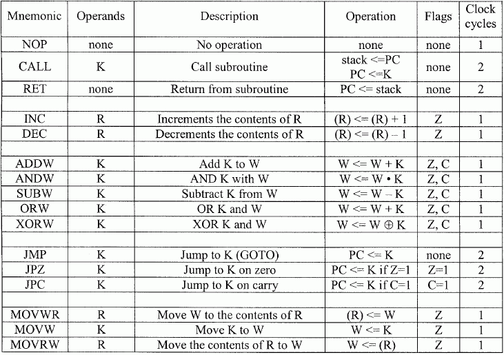
The Instruction Set - This is an extract from the AQA exam data sheet.

Understanding This Chart
- This all looks unfamiliar.
- It is a shorthand notation for some very simple steps so Don't Panic!
- There is some obscure language which is easy once you get the hang of it.
A beginner's Example
- The processor contains a register named "W", the working register. This is just a box where you can store a number.
- There is a Mnemonic named ADDW. This command adds a number to the one stored in "W".
- ADDW has one operand. This is the number that is going to get added to the one in "W".
- If you want to add "1", the simulator expects all its numbers to be in Hexadecimal format so you have to type 0x1.
CTRL+Click here to run the simulator.
- Type in the code below or copy and paste it.
- Click the "A" button to assemble the code (translate it into binary).
- Click the "S" button to step through the program.
   ADDW 0x1
   ADDW 0x2
   ADDW 0x3
- ADDW is the mnemonic.
- 0x1 is the operand.
- click the "A" button to assemble the code (translate it from the human readable form into binary, understood by the processor).
- click the "S" button to step through the program. You will need three clicks.
- watch what happens to the "W" register. This is located near the top left of the simulator screen.
- "W" contained zero, then one, then three and finally six.
- if you missed any of the detail, click "A" again to reset everything and click "S" three more times.
All that Jargon and effort to work out that 0 + 1 + 2 + 3 = 6
Mnemonics
- Each of the sixteen commands has its human readable, easily remembered mnemonic.
- Each mnemonic represents a very unmemorable binary code understood by the processor.
- Without the mnemonics, you'd have to learn and use the binary codes.
- The original programmers of the very first computers had to use the raw binary codes!
- The ASSEMBLER program made life much easier by translating the human readable mnemonics into binary.
Operands
- The commands perform simple tasks.
- The operand is used by the command to complete its task.
- In the example above, the operands were just numbers that were going to get added to "W".
- The other commonly used operand is the file register number where data is going to be fetched or written.
Description
This is a brief explanation of what the command does.
Operation
- If you know that <= means "is copied to", this column becomes clearer.
- The direction of the arrow shows what is copied and where the answer goes.
- Some commands look as though something is copying into itself. For example ADDW ...
- W <= W + K
- This means add K to W and copy the new answer into W. The original data in W is overwritten.
- K is the operand.
Flags
The processor has a Status Register (SR) containing three flags. The table above shows which flags might be set by each command.
- C is the carry flag. This binary digit is set to one if a calculation gives a result too big to fit in eight bits.
- T is the timer flag. This is set when the timer reaches zero after counting down.
- Z is the zero flag. This is set when a calculation, logic operation or move leaves zero in the working register "W".
Clock Cycles
- Most commands take one clock cycle to finish.
- The exception to this rule is commands that change the Program Counter register, PC.
- This register keeps track of which instruction the processor is working on.
K and (R)
- K is usually just a number. For example in this command ...
- ADDW 0x1 W <= W + K
- K represents the number 0x1
The microcontroller has 256 memory locations called the File Registers.
- (R) in plain English is read as "the contents of file register R".
So the command MOVWR 0x12 (R) <= W means copy W into the contents of file register 0x12.
The simulator instruction set matches the AQA specification very closely. AQA did not specify the binary level details of the processor so this simulator uses binary codes which are very like those used in the Microchip family of microcontrollers.
The code is NOT case sensitive so movw is the same as MOVW and 0XFF is the same as 0xff.
Most features in the AQA specification are now available in the simulator.
Some design assumptions have been made so the exam microcontroller might differ from this one.
Literals
K is used to represent a literal, which can be
- a memory location (e.g. 0x29),
- a label (e.g. display:) or
- a value, (e.g. 0xFA).
- Legal literal names begin with _ or a text character.
- Literal names must not begin with a digit and must only contain _ : a-z A-Z 0-9.
- Literal names must not duplicate reserved words such as MOVW or CALL.
- Literal names must be unique or the assembler will not be able to resolve the ambiguity.
File Registers
R represents a register or memory location.
Differences between this simulator and the AQA version.
INC potentially sets both the Z and C flags. AQA only sets the Z flag.
DEC potentially sets both the Z and C flags. AQA only sets the Z flag.
Non AQA Extras
Define Byte - DB - Variables
The AQA "Changes to Content" document describes the use of literals as both labels and values. But it does not have a way to define them in a program. Many assembler languages use DB for this purpose so it has been added as an extra to the AQA instruction set. In high level languages, these named memory locations are called variables.
Using DB, it is possible to name a memory location and refer to the contents of the location by name. In addition, data can be stored using DB, even if the memory location is not labelled but this is poor programming style as the program is less easy to understand.
Run this example and watch how the named memory locations get initialised when the program is assembled and how they change when it's run.
        JMP     START

; ===== NAMED DATA LOCATIONS =====
DELAY:  DB      0x55    ; Address 1
COUNT:  DB      0x10    ; Address 2
        DB      0xAA    ; Address 3

; ===== THE MAIN PROGRAM =====
START:
        INC     DELAY   ; Add 1
        DEC     COUNT   ; Subtract 1
        INC     0x03    ; Poor style
        JMP     START
; ============================
reviseOmatic V3
Contacts, ©, Cookies, Data Protection and Disclaimers
Hosted at linode.com, London
